


PCB Layout Services – Precision Engineering for Reliable and High-Performance Electronics
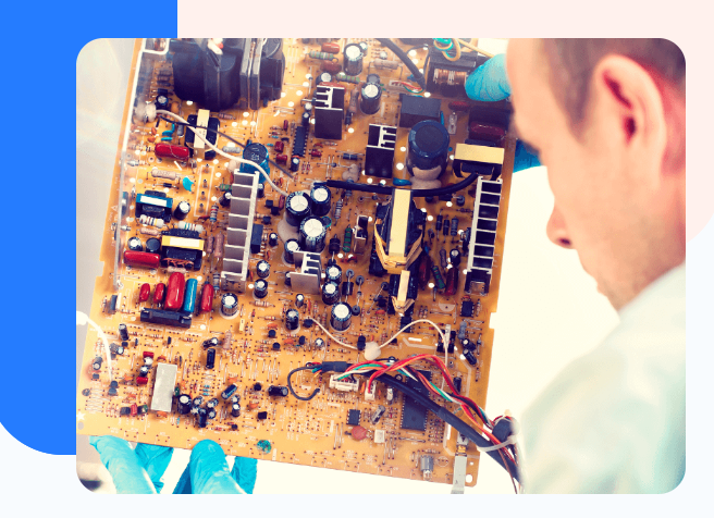
In the modern electronics industry, PCB layout services are a critical step in transforming circuit ideas into fully functional, manufacturable, and high-performance hardware products. Every electronic device—from smartphones and medical equipment to industrial controllers and IoT systems—relies on a well-designed printed circuit board (PCB) to function correctly.
A professional engineering firm like Wagner Engineering provides advanced PCB layout services that ensure optimal component placement, precise routing, and manufacturable designs tailored for complex embedded and electronic systems. Their expertise spans PCB design, firmware development, embedded systems, and cloud integration, enabling complete end-to-end engineering solutions.
What Are PCB Layout Services?
PCB layout services refer to the process of converting an electronic schematic into a physical board design that can be manufactured and assembled. This includes arranging electronic components on the board, routing electrical connections (traces), and ensuring the design meets electrical, mechanical, and manufacturing requirements.
In simple terms, PCB layout is the stage where an abstract circuit diagram becomes a real-world, buildable product. According to industry definitions, PCB layout services produce fabrication-ready files such as Gerber data, drill files, and assembly drawings used by manufacturers to produce the final board.
Why PCB Layout Services Are Important
PCB layout is not just about placing components—it is a highly technical engineering process that directly affects product performance, reliability, and cost.
1. Ensures Signal Integrity
Proper layout ensures that signals travel through the board without noise, distortion, or interference. This is especially important for high-speed and RF circuits.
2. Reduces Electromagnetic Interference (EMI)
Poor routing can cause unwanted electromagnetic noise. A professional layout minimizes EMI through controlled trace routing and grounding techniques.
3. Improves Thermal Performance
Component placement and copper distribution are optimized to manage heat efficiently, preventing overheating and system failure.
4. Enhances Manufacturability
Good PCB layout ensures the design can be manufactured easily, reducing production errors and cost.
5. Increases Product Reliability
A well-designed PCB reduces failure rates and ensures long-term stable performance in real-world conditions.
Core Elements of PCB Layout Services
A complete PCB layout process involves several engineering stages:
1. Component Placement
Engineers strategically place components to minimize signal path lengths and optimize performance.
2. Board Stack-Up Design
The number of layers and their arrangement (power, ground, signal layers) are defined to ensure electrical stability and impedance control.
3. Trace Routing
Electrical connections are carefully routed to maintain signal integrity, especially for high-speed or sensitive signals.
4. Via and Layer Management
Vias are used to connect different layers, and their placement is optimized for performance and reliability.
5. Design Rule Checks (DRC)
Automated and manual checks ensure the design meets electrical and manufacturing constraints.
6. Output File Generation
Final outputs include Gerber files, BOM (Bill of Materials), and assembly drawings for manufacturing.
PCB Layout vs PCB Design
It is important to distinguish between PCB design and PCB layout.
- PCB design focuses on circuit functionality, schematic creation, and selecting components.
- PCB layout focuses on the physical placement and routing of those components on the board.
Both stages are essential, but PCB layout is where theoretical design becomes a real, manufacturable product.
Role of PCB Layout Services in Modern Electronics
With increasing demand for compact, high-speed, and intelligent electronic devices, PCB layout services have become more important than ever.
They are widely used in:
- Consumer electronics (smartphones, wearables, smart devices)
- Automotive systems (ECUs, sensors, infotainment systems)
- Industrial automation (robotics and control systems)
- Medical devices (monitoring and diagnostic equipment)
- IoT systems (connected smart devices)
Modern systems require compact layouts, high-speed routing, and multi-layer designs to support advanced functionality and miniaturization.
Benefits of Professional PCB Layout Services
Working with an experienced engineering company provides several advantages:
1. Expert-Level Design Accuracy
Engineers ensure that every trace, component, and layer is optimized for performance.
2. Faster Product Development
Professional workflows reduce redesign cycles and accelerate time-to-market.
3. Lower Manufacturing Costs
Optimized layouts reduce errors, rework, and production waste.
4. Improved Electrical Performance
Signal integrity, power distribution, and grounding are carefully engineered.
5. Better Product Longevity
Reliable layouts ensure stable performance over long-term use.
Wagner Engineering – PCB Layout Services Expertise
Wagner Engineering is a multidisciplinary engineering company offering PCB layout services, PCB design, firmware development, software engineering, and cloud application development. Their integrated approach ensures that hardware and software work seamlessly together for optimal system performance.
Their PCB layout capabilities include:
- High-speed and multi-layer PCB layout design
- Signal integrity and impedance-controlled routing
- Power distribution and thermal optimization
- Design for manufacturability (DFM) compliance
- Integration with embedded firmware and systems
This holistic engineering approach ensures that every PCB is not only functional but also optimized for real-world manufacturing and performance.
Future of PCB Layout Services
The PCB layout industry is evolving rapidly with technological advancements:
- AI-assisted PCB routing and optimization
- High-density interconnect (HDI) designs
- Flexible and wearable electronics
- Increased use of automation tools
- Integration with IoT and cloud-based systems
These advancements are making PCB design faster, more accurate, and more efficient than ever before.
PCB layout services are a fundamental part of modern electronics development, ensuring that circuit designs are transformed into reliable, efficient, and manufacturable hardware products. From component placement to signal routing and thermal management, every detail plays a crucial role in product success.
With expertise in PCB design, embedded systems, and complete engineering solutions, Wagner Engineering delivers advanced PCB layout services that help businesses bring high-performance electronic products to market with precision and reliability.
- Digital Agency
- Literie
- Location de voitures
- Restaurant
- Restaurant
- Mode
- Mode
- Information
- Marketing
- Tourisme
- Développement
- Découverte
- Législation
- Gastronomie
- Pâtisserie
- Event
- Art
- Causes
- Crafts
- Dance
- Drinks
- Film
- Fitness
- Food
- Παιχνίδια
- Gardening
- Health
- Κεντρική Σελίδα
- Literature
- Music
- Networking
- άλλο
- Party
- Religion
- Shopping
- Sports
- Theater
- Wellness
 Greek
Greek
 Indian
 English
 French
 Arabic
 Spanish
 Portuguese
 Deutsch
 Turkish
 Dutch
Dutch
 Italiano
 Russian
 Romaian
 Portuguese (Brazil)